Ansys Lumerical MODE
Whether your prototype is focused on fiberoptics or consolidated photonics, MODE has everything engineers require to optimize waveguide and coupler designs.
Whether your prototype is focused on fiberoptics or consolidated photonics, MODE has everything engineers require to optimize waveguide and coupler designs.
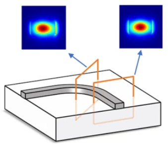
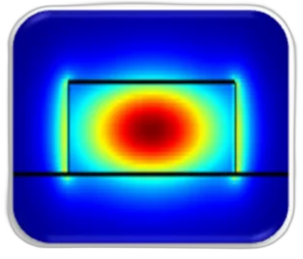
Engineers can reliably predict waveguide and coupler performance using Ansys Lumerical MODE.
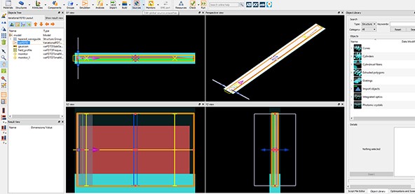
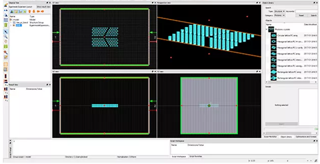
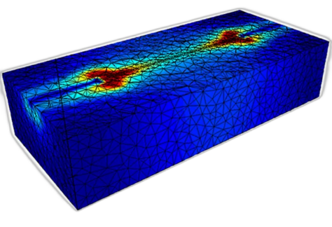
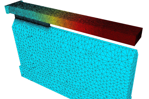
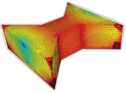
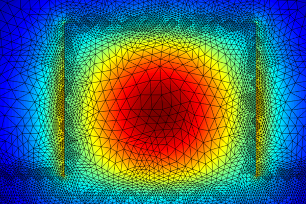
Large planar structures and extended propagation lengths are no problem for MODE, which combines bidirectional Eigenmode expansion, varFDTD, and finite difference eigenmode solvers to deliver accurate spatial field, modal frequency, and mode overlap evaluations.
Functionality and practical industrial application


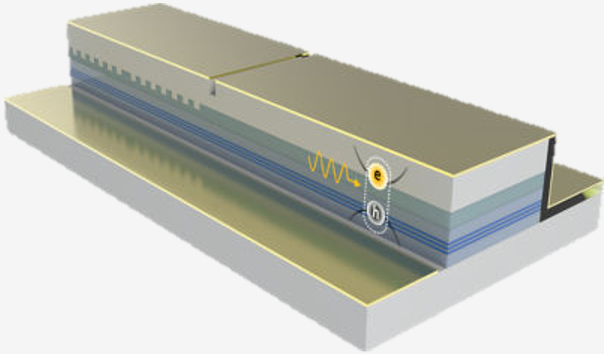
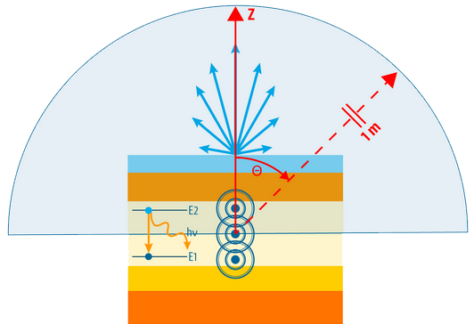
Designers can model interacting optical, electrical, and thermal effects thanks to tools that seamlessly integrate device and system level functionality. A variety of processes that combine device multiphysics and photonic circuit simulation with external design automation and productivity tools are made possible by flexible interoperability between products.