Ansys PathFinder-SC (Semiconductor)
Ansys PathFinder-SC is a high-capacity solution to help you plan, verify and sign-off IP and full-chip SoC designs for integrity and robustness against electrostatic discharge (ESD).
Ansys PathFinder-SC is a high-capacity solution to help you plan, verify and sign-off IP and full-chip SoC designs for integrity and robustness against electrostatic discharge (ESD).
Ansys Pathfinder-SC, verification, sign-off IP and full-chip SoC designs for integrity and performance. In addition, the software also identifies design issues that can cause chip or IP failure from charged-device model (CDM), human body model (HBM) or other related ESD events.
Ansys PathFinder is signoff certified by all major foundries, ensuring that interconnect parasitics, HBM/CDM ESD automation and current-density checks are silicon accurate. It’s layout-based GUI facilitates rapid root cause detection and intuitive debugging interfaces.
Pathfinder Core Features Include:

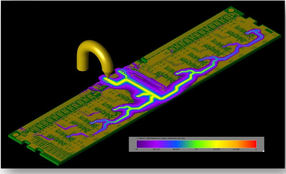
PathFinder-SC imitates human body model (HBM) and charged-device model (CDM) ESD events by propagating the zap current. That is, Electrostatic Discharge (ESD) through power/ground networks to isolate layout bottlenecks. The software models the injection of current into any pad and interconnect pathway to identify pin-clamp-pin paths that can’t handle or regulate high ESD currents.

