Abstract
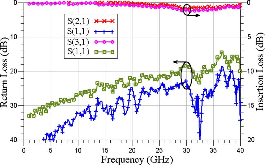
The types of RF MEMS devices proposed are latching RF MEMS switches: Single-Pole-Single-Throw (SPST), Single-Pole-Double-Throw (SPDT), and Single-Pole-Triple-Throw (SP3T). The switches are built with a 20 μm thick nickel layer covered with a plated 2 μm gold layer on the top and side walls of the nickel, eliminating potential warping due to thermal mismatch. The switches are actuated using a high-stroke latching thermal actuator that exhibits a 32 μm displacement with a DC power of 250 mW under ambient pressure at 25°C (298 K) and 153 mW under vacuum at -80°C. The measured velocity for the actuator is 2.3 mm/s. The RF measurement of the SPST switch is performed under ambient and vacuum conditions over a wide range of temperatures from 25°C (298 K) to -80°C. The switches survived a temperature cyclic test from 25°C to 85°C (358 K) with a total variation of 0.2 dB in insertion loss. The switch demonstrates a worst IP3 (third-order intercept point) of 60.14 dBm and high-power handling capability exceeding 30 W, tested for one hour in one cycle. The RF performance of the SPST, SPDT, and SP3T exhibits a worst insertion loss of 0.8 dB, 1.2 dB, and 1.5 dB up to 40 GHz, 40 GHz, and 18 GHz, respectively.
Introduction to MEMS Device Technology
RF MEMS switches have the potential to replace semiconductor switches due to their lower loss, better linearity, and better RF performance. Due to MEMS technology advances over the past decade, several MEMS switch concepts have been introduced to overcome issues related to RF performance, actuation voltage, reliability, and power handling capability. RF MEMS switches can be classified based on the actuation concept implemented in such switches. There are switches based on electrostatic actuators, thermal actuators, and piezoelectric actuators. In comparison between electrostatic actuation and piezoelectric actuation, electrostatic seems to be easier to implement than piezoelectric. Electrostatic actuator types demonstrate compact size and good RF performance; however, they handle relatively lower RF power and suffer from self-actuation. On the other hand, thermally actuated RF MEMS switches use thicker layers than electrostatic switches, making them less sensitive to thermal conditions imposed by the surrounding environment, and they have the potential to handle higher RF power with no self-actuation. Nevertheless, thermal switches suffer from high DC dissipated power.
Commercially available mechanical bistable switches eliminate the DC power consumption after achieving the stable state. However, these switches are bulky and very heavy. In order to achieve a similar performance in thermally actuated RF MEMS switches, a mechanical latching mechanism had to be developed. Although electrostatically actuated switches do not effectively consume DC power, they suffer from stiction and dielectric charging problems. Thermal actuators are not sensitive to these problems. Additionally, the ability to design stiffer thermal actuators minimizes issues resulting from fatigue and arcing, especially when the switch is meant to work in a hermetically sealed package with the existence of non-active gases.
Unlike previously published latching RF MEMS switches, the proposed switches can operate under vacuum and over a wide range of temperatures down to -80°C, making them compatible with hermetically sealed vacuum packaging and operation at cryogenic temperatures. The developed actuator for the proposed switches does not rely on the thermal conduction phenomena in the air between the actuator and the thermal heater, as seen in other designs. Also, being fabricated from relatively stiff material, 20 μm thick nickel, makes it resistant to warping due to mismatches in the thermal expansion coefficient in thin-film layers.
MEMS Device Actuator Design and Speed Measurement
A MEMS device thermal actuator that exhibits high lateral stroke is designed, fabricated, and measured. The actuator is built using the MetalMUMPs process from MEMSCAP Inc. The cross-sectional view of the MetalMUMPs process shows the layers used. The process consists of two conducting structural layers, nickel and poly-silicon, and two dielectric layers of silicon nitride on high resistive silicon substrate, with the capability of having a trench in the silicon substrate underneath the designed device.
Unlike previously published actuators, this actuator is designed to work in atmospheric pressure and vacuum. It does not rely on air as the medium to transfer heat from the heater to the nickel metal layer. Instead, the heater, built from the poly-silicon layer, is in direct contact with the nickel through a nitride layer, with no air gap. The heat transferred from the poly-silicon through the nitride to the nickel results in deformation due to the heated nickel. This design allows the actuator to function in vacuum as well.
The actuator’s nickel arrays are laid out with a slight tilt angle, such that heat from the poly-silicon resistor causes expansion due to the thermal expansion coefficient of the nickel. The anchored side of the arrays does not move, but the suspended sides move in opposite directions. This tilt angle favors displacement in the desired direction.
The speed of the actuator used in the RF MEMS switches is measured using a custom setup. Two pads, located 32 μm apart, are used as sensors to detect the time the actuator takes to achieve maximum displacement. The measured time to achieve a 32 μm displacement is found to be 14 ms, and the corresponding velocity is 2.3 mm/s.
Single Pole Single Throw (SPST) Switch Design
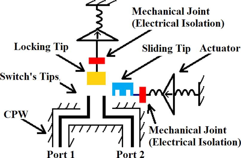
The proposed switch consists of two tips that are mechanically anchored to the substrate and represent the switch’s two electrodes. The two moving tips, as shown in Figure 1, are responsible for closing and opening the switch through a latching cycle driven by two thermal actuators.
The first moving tip is called the “sliding tip,” which is responsible for making contact with the switch’s two tips by inserting them into the grooves. The second moving tip is called the “locking tip,” and its function is to apply lateral force on the sliding tip, pushing it against the switch’s tips to ensure a solid contact force. The simulated contact force applied by the locking tip on the sliding tip is found to be 3.2 mN. The switch is designed to be closed when the sliding tip makes contact with the switch’s tips and locked by the locking tip. It opens when the sliding tip is not in contact with the switch’s tips. Both moving tips are independently mounted on separate thermal actuators.
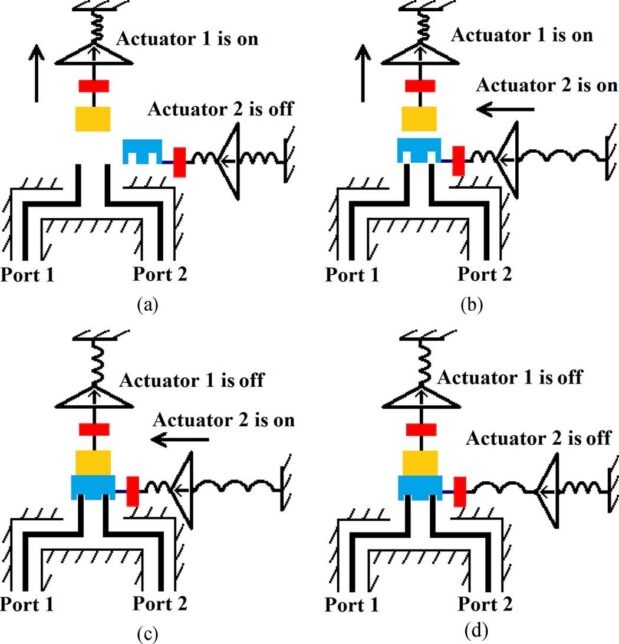
The switch is latched in four sequential steps as shown in Figure 2. First, the locking tip is pulled away to clear the path for the sliding tip (Actuator 1 is on, Actuator 2 is off) (Figure 2a). In the second step, the sliding tip is pushed forward so that its grooves align with the switch’s sharp tips (Actuator 1 is on, Actuator 2 is on) (Figure 2b).
In the third step, the actuator of the locking tip is released to push the sliding tip into contact with the sharp tips (Actuator 1 is off, Actuator 2 is on) (Figure 2c). Finally, the sliding tip’s actuator is released, applying a lateral force perpendicular to the lateral force from the third step (Actuator 1 is off, Actuator 2 is off) (Figure 2d).
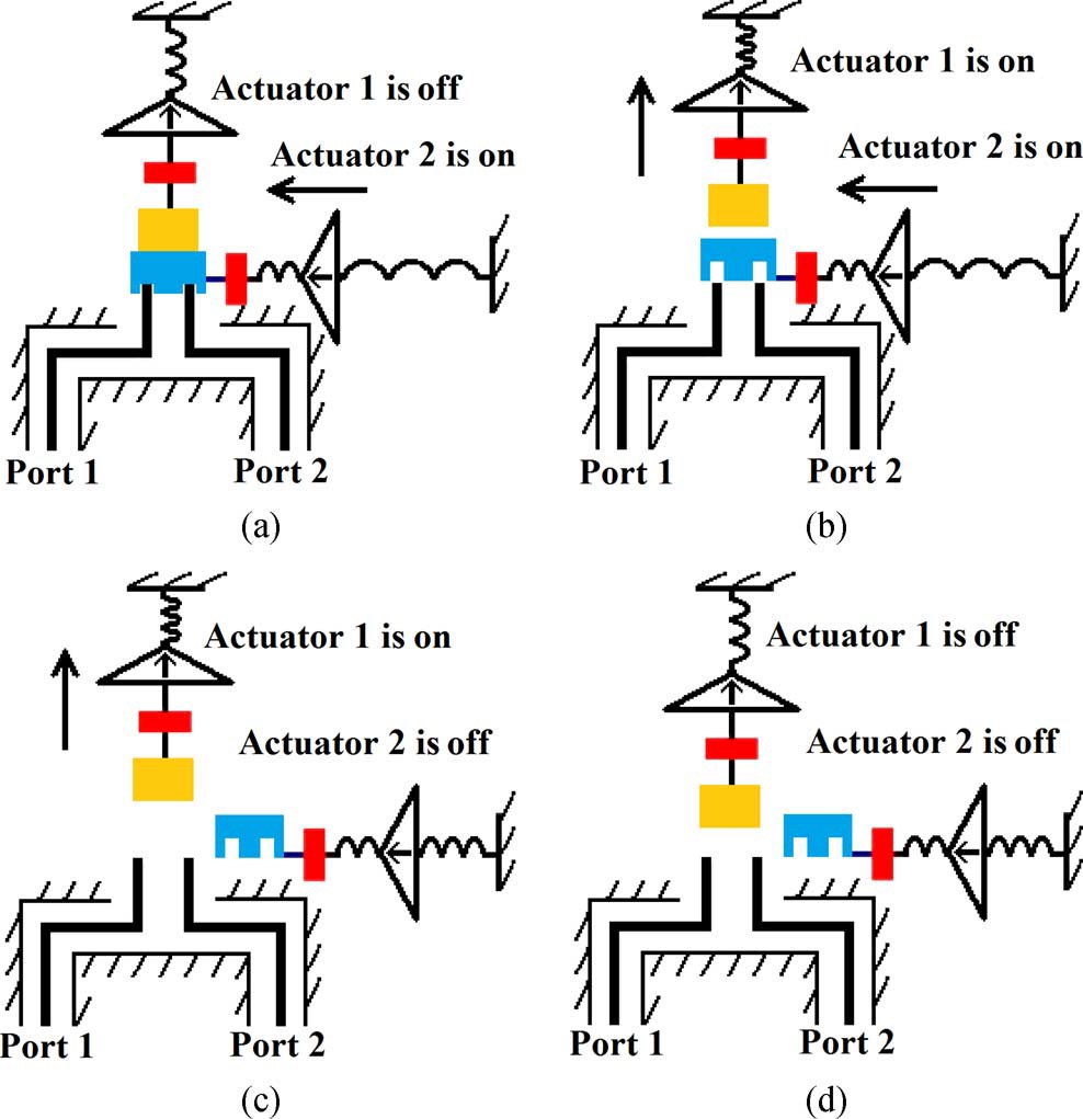
The unlatching process reverses the latching steps, as shown in Figure 3, and both latching and unlatching are achieved by manually applying actuation voltages.
Simulation, RF, and Low Temperature Measurement in MEMS Devices
The MetalMUMPs process exhibits one metal layer made of nickel, top plated with gold. A second gold plating can be applied on the sidewalls of the nickel layer. To access the two tips of the proposed RF MEMS switch, an opening must be made to one side of the CPW. To compensate for the RF performance loss due to this opening, a modified CPW topology was developed in the proposed RF MEMS design. A conventional CPW was designed using Ansys HFSS, achieving an RF response of 0.4 dB insertion loss and better than 25 dB return loss at 40 GHz. The designed distances for the center conductor and gaps were 24 μm and 26 μm, respectively, with a metal thickness of 20 μm.
In order to access the central conductor of the RF MEMS switch, one side of the CPW ground was cut, creating a degradation in the RF response. A two-wire bond was introduced to fix the ground defected CPW (GDCPW) RF response. However, the two wire bonds increased the total inductance of the GDCPW, requiring tuning of the distances using parametric simulation in HFSS. The new distances for the center conductor and gap were 24 μm and 18 μm, respectively, with the same thickness. The increased capacitance compensated for the increased inductance. Simulation results of the GDCPW and conventional CPW show similar RF performance, with a worst insertion loss of 0.44 dB at 40 GHz.
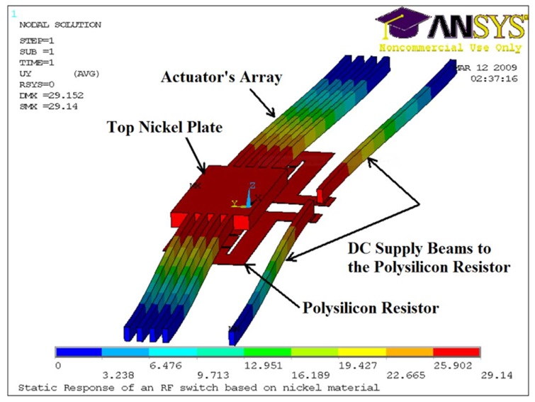
Three tests were carried out on the proposed switch. First, the switch was measured at Standard Ambient Temperature (25°C) and Pressure (SATP) using a Cascade RF probe station. The switch was closed and latched using a 32 μm displacement. The measured voltage and current to achieve this were 12 V and 21.21 mA, respectively, consuming 250 mW of DC power. Figure 4 illustrates the Finite Element Method simulation that was carried out using Ansys software. The model included the effects of the substrate, and ambient temperature and pressure.
Second, the switch was tested under vacuum using a cryogenic RF probing station at SATP. The measured voltage and current were 9.5 V and 16.12 mA, consuming 153 mW of power. The switch was also tested at -80°C under vacuum, showing no significant difference in DC power consumption. Under vacuum, the switch’s power consumption was reduced due to the excellent thermal isolation provided by the vacuum environment.
Lastly, the switch was simulated in HFSS up to 26 GHz. Measured insertion loss and return loss under vacuum and cryogenic conditions were compared to the simulation, with a maximum displacement of 40 μm achieved with 175 mW of power under vacuum.
RF MEMS High Temperature Measurement
Temperature cycling is performed on the proposed switch between Standard Ambient Temperature (SATP) and 85°C (358 K) under ambient pressure. The S-parameters of the switch are measured at room temperature 25°C (298 K), then the switch is heated up to 85°C (358 K), and the S-parameters are measured again. The switch is cooled back to room temperature, and a third measurement is taken. The switch is opened, closed, and latched at the end of the third measurement. This procedure is repeated for several cycles.
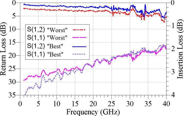
After testing the switch for several cycles, no permanent degradation in RF performance was observed. However, there was a temporary variation of 0.2 dB in insertion loss and 3 dB in return loss at 20 GHz due to the change in operating temperature. Different contact points between the sliding tip and the switch’s tips are also believed to contribute to the RF performance variation. The best and worst RF performance obtained from temperature cycling are shown in Figure 5.
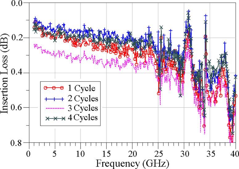
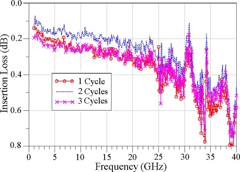
The extracted contact resistance varied between 2.4 Ω and 1.2 Ω at 25°C (298 K) under ambient pressure, while at 85°C (358 K), it varied between 1.8 Ω and 1.2 Ω, as shown in Figures 6 and 7, respectively. The variation in insertion loss at 85°C (358 K) was less than at 25°C (298 K), which may be related to the softening of gold at higher temperatures.
Single Pole Double Throw (SPDT) Switch
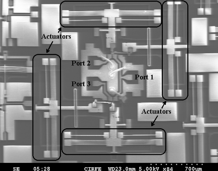
The second proposed RF MEMS switch is a SPDT switch based on the GDCPW topology. The switch uses four of the developed thermal actuators to construct two switchable paths. The top view of the SEM picture of the developed SPDT, including the thermal actuators, is illustrated in Figure 8.
The switch uses the CPW topology and has two defects in the ground planes of the CPW outer sides. These defects make an opening in the ground, allowing access to the switch’s tips through laterally actuated sliding and locking tips to perform the close and open states of the RF switch.
The latching and unlatching phenomena are also achieved using the same technique mentioned for the SPST switch. Wire bonds are used to bridge the defected ground to improve RF performance. As a result of this bonding, the insertion loss and return loss of the fabricated switch are enhanced. The RF performance of the proposed SPDT switch is measured and illustrated in Figure 9.
Single Pole Triple Throw (SP3T) Switch
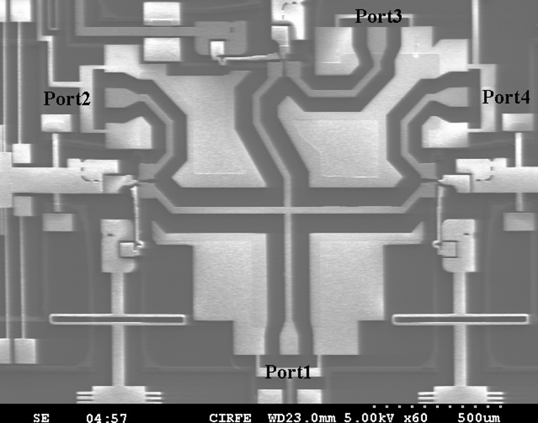
The third type of the proposed switches is the SP3T switch that routes the signal to three paths. As depicted in Figure 10, the switch has 50Ω adaptors that transform the high characteristic impedance to a 50Ω characteristic impedance. The top view of the SEM picture of the SP3T is shown in the same figure.
Advanced Design System (ADS) from Keysight is used to optimize the RF performance of the proposed switch. The trade-off in the SP3T design is a reduced upper frequency due to the high loading from the relatively long paths of the other two that are kept open.
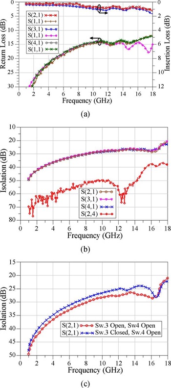
As illustrated in Figure 11(a), the SP3T switch exhibits a worst insertion loss of 1.6 dB and a return loss of 12 dB for one closed path at a time of the three paths. The worst isolation between all ports is 20 dB, as shown in Figure 11(b), while all switches are open. The isolation between ports 2 and 4 is higher than the other ports since there are two switches in series, resulting in a smaller coupling capacitance. The isolation between port 1 and port 2 is measured when switch number 3 for port number 3 is closed, as illustrated in Figure 11(c). The isolation over the whole range remains better than 20 dB.
Conclusion
The high-power latching RF MEMS devices discussed in this blog, including SPST, SPDT, and SP3T types, demonstrate superior RF performance with minimal insertion loss, high power handling, and robustness across varying temperature conditions. The use of a nickel-gold structure and a thermal actuator with a high lateral stroke ensures durability and efficiency, even in vacuum and cryogenic environments. The proposed designs offer promising solutions for high-performance RF switching applications, presenting significant improvements over existing technologies in terms of power consumption, linearity, and temperature resilience.
Ready To Bring Your RF Designs To The Next Level?
Connect with our expert electromagnetics engineers to explore how our design and simulation services can align with your unique needs. Whether it’s custom solutions or powerful simulation software, we’re here to help optimize your next innovation. Contact us today and start transforming your ideas into reality!

Maher Bakri-Kassem, PhD, PEng
Senior Electrical Consulting Engineer, SimuTech Group
Maher Bakri-Kassem has over 20 years of experience in Low Frequency, RF/microwave, and semiconductor (including MEMS) R&D across industry and academia. He has worked on applications like RF MEMS switches, varactors, RF circuits, optical MEMS, microfabrication processes, and MEMS/CMOS integration, with expertise in mass production and packaging. Maher also has 2 years of experience in satellite systems, specializing in uplink earth stations and VHF/UHF hardware. He is skilled at problem-solving, authored over 40 publications, and holds a patent on RF MEMS/CMOS integration.
The preceding blog post is an adapted summary of the whitepaper titled “High Power Latching RF MEMS Switches” written by Maher Bakri-Kassem, Senior Member, IEEE, and Raafat R. Mansour, Fellow, IEEE, and published in IEEE Transactions on Microwave Theory And Techniques, Vol. 63, No. 1, January 2015. For a deeper dive into the technical details and full analysis, we encourage you to review the original whitepaper.


