Introduction to Photonic Integrated Circuits (PIC)
For photonic integrated circuit (PIC) chip designers, it is important to be aware of the interoperability of simulation tools. Simulations may be the key to cutting-edge devices, but the capability to translate designs from simulation software into error-free, foundry-compatible blueprint files is also crucial to actualize the product.
The blueprint format, often referred to as the layout, has strict rule sets that vary between foundries. Although it is feasible to manually draw a layout, it can quickly become a Herculean task as photonic integrated circuits become more complex.
Hundreds of thousands of devices can fit within the average PIC chip. Thus, it is often unreasonable to draw and validate the layout manually.
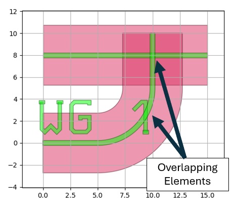
Example of using layout operations to detect and highlight overlapping elements in a photonic integrated circuit (PIC) design.
Luceda Photonics empowers photonic engineers with Luceda IPKISS, an integrated design platform for efficient and scalable photonic circuit development.
Generating PIC Layouts
Ansys Lumerical offers a large variety of choices for photonic integrated circuit layout generation. One of the popular electronic-photonic design automation (EPDA) tools with Ansys Lumerical integration is Luceda IPKISS. Luceda IPKISS is a python-based platform that enhances PIC design flows. Luceda IPKISS provides features for parametric PIC design and layout automation, design validation, and tape-out preparation.
Using the Lumerical and Luceda IPKISS tools together, designers can bundle their simulation into parameterized cells, also referred to as “Pcells”. Pcells are in essence Python class files that help compartmentalize design information or simulation results that are specific to the device. This can include parameters, cell geometry, cell hierarchy, simulation automation, and simulation results (s-parameter files).
With the Pcell, designers now have a one-stop location for all their design needs. At first glance, designers can input parameter values and instantly produce the device geometry. Next, an automated simulation can be generated and ran to produce performance information, such as the device transmission. Previously calculated simulation results or experimentally measured metrics can also be bundled with Pcells for quick access. When performing signal integrity analysis, multiple Pcells are connected to simulate the expected circuit response.
With a finalized design, Pcells can be invoked to efficiently produce layout schematics, removing the need to draw the layout manually. For example, users can instantiate a device, specify the ports to connect, and generate the layout file, all within a few lines of Python code as shown below:
#Initialize Devices
CDC = CDC.ContraDC() #contra-directional coupler device
GC = pdk.GratingCoupler() #grating coupler device
insts = {
"CDC1":CDC,
"GC1": GC,
"GC2": GC,
} #instances of the devices

#Place and Connect
specs = [
    i3.Place("CDC1", (50, 127*1.5),angle=90),
    i3.Place("GC1",(0,0)),
    i3.Place("GC2",(0,127)),
    i3.ConnectBend("GC1:out","CDC1:Port1"),
    i3.ConnectBend("GC2:out","CDC2:Port2"),
]

#Create Circuit object and generate layout
my_circuit = i3.Circuit(
    name="example_layout",
    insts=insts,
    specs=specs,
    exposed_ports=exposed_port_names,
)
my_circuit_layout.Layout().write_gdsii("example_layout.gds") #generate layout
A concise tutorial about the Lumerical and Luceda IPKISS interoperability is available through SimuTech Skill Center.
Validating Your Photonic Integrated Circuit with DRC
To successfully submit a PIC layout file to a foundry, the layout must be fully error free based on the criteria of the foundry. These requirements are referred to as “Design Rule Checks (DRC)” and foundries will often provide their own DRC rule decks for customers. As the rules are numerous and comprehensive, foundries will often also have available DRC rule decks in formats of proprietary software that are popular in the industry.
Below we showcase some common validations that are automated with Luceda IPKISS. It is also possible to run DRC using the Luceda Link for Check Mate DRC. Users can run DRC to check their layout against the rule decks provided by their foundry. Please note that Luceda Link for Ansys Lumerical is also available to enhance your physical simulation flows, define your layouts and simulation recipes in Luceda IPKISS, and run them using Lumerical FDTD or EME.
A common mistake when generating layouts with interconnects are overlapping devices. Especially in the design of passive photonic circuits, this type of mistake is commonly missed because layer rules are not always violated when overlaps occur.
Luceda IPKISS provides a functionality to detect all overlapping elements and collect them in a Python dictionary object. The potentially problematic areas can also be highlighted when viewing the layout within the command line. Additional customization is also possible to cater to specific use-cases.
Image courtesy of Luceda Photonics
This is one of the most unexpected layout errors when layouts are generated. Designers often may not realize that a geometry is unrealistic when performing simulations. Although the ideal shape is sought after as it can provide the theoretical best performance, it is important to consider the performance trade-off to ensure a device is feasible to fabricate.
In other cases, sharp angles may have been unforeseen while designing the PIC, such as the example shown below where a directional coupler was created from two bent waveguides and their respective cladding layers had overlapped to form the DRC error.
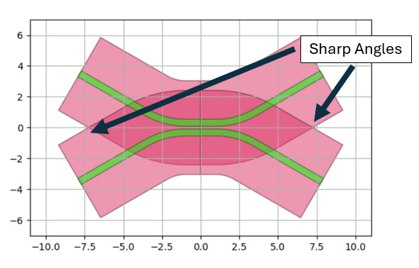
Similar to the overlapping elements functionality, Luceda IPKISS provides users a function to detect all acute angles. Users can then utilize a special feature to create ‘stubs’ – small structures that plug up the angles to alleviate the DRC error.
Image courtesy of Luceda Photonics
All commercial foundries prescribe rules that submitted layouts must adhere to. These rules typically address topics such as minimum allowable distances between features, minimum feature sizes, and unallowable layer overlaps. World-class foundries enable their DRC in one or more DRC software packages so users can run DRC themselves and submit error-free layouts for fabrication (or, if a user will accept some risk in their layout, they might choose to waive certain DRC errors if approved by the foundry).
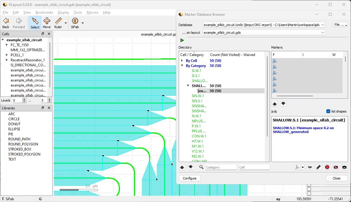
Luceda provides the ability to run DRC from KLayout or from Check Mate DRC, depending on the foundry. Both DRC tools provide a tree list of all areas checked by the DRC as seen in the image above. Satisfactory results are labelled in green while problematic areas are labelled in red. Users can click through the DRC violations and the viewer will jump to each location with a box that highlights the checked feature.
Image courtesy of Luceda Photonics
Simulation to Success
Ansys software provides a wide range of interoperability and empowers teams with the tools needed to create quality products. Whether it is mechanical stress, thermal heating, or electrical-optical effects, engineers are geared with a simulation repertoire that meets the challenge.
Photonics continues to rapidly advance alongside technologies such as Quantum, AI, VR/AR, and LiDAR. Consequently, tools such as Ansys Lumerical enable efficient workflows resulting in decreased time to market are an invaluable competitive edge.
Ready to Take Your Photonic Integrated Circuit Design to the Next Level?
Explore SimuTech Group’s photonic simulation consulting services and discover how we can help you turn your vision into reality on time, on budget, and with unparalleled precision. Contact us to connect with a simulation expert today!
For questions about Luceda IPKISS, visit the Luceda Photonics Design Platform to learn more.

Stephen Lin, MASc, Electrical Engineering/Silicon Photonics
Photonics Staff Engineer, SimuTech Group
Stephen Lin has six years of experience in Silicon Photonics design and PDK development and is well-versed in industry standard software, including Ansys Lumerical, Ansys Zemax OpticStudio, Mentor Graphics Pyxis & Calibre, and SiEPIC PDK/Tools. He is skilled in foundry submission process (DRC, foundry layers, etc.), and has long-time interest in multi-physics and co-simulation of photonic systems.