The AEDT Mechanical solver gives RF engineers a way to study stress, strain, deformation, and thermal effects directly within the Ansys Electronics Desktop environment. While HFSS and SIwave are well known for electromagnetic and signal integrity simulations, AEDT also provides a Mechanical solver that is especially important for advanced packaging, solder joints, and PCB assemblies, where mechanical reliability is as critical as electrical performance.
In this article, we review the basic principles of stress and strain, the setup of a mechanical simulation in AEDT, and how to use parametric sweeps to evaluate warpage and stress distribution across temperature ranges.
Fundamental Concepts: Stress and Strain for the AEDT Mechanical Solver
Stress and Strain
-
Stress (σ): Defined as force per unit area.
-
Strain (ε): Defined as the relative change in length, ΔL/L.
In the elastic region, stress and strain are related by Hooke’s Law:
where E is the Young’s modulus.
Shear Stress and Shear Strain
Shear stress (τ) and shear strain (γ) follow a similar linear relationship:
where G is the shear modulus.
Stress–Strain Curve
-
In the elastic region, the material returns to its original shape when the load is removed.
-
Beyond the yield point, the material enters the plastic region, where permanent deformation occurs.
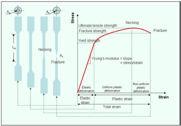
Ref1.
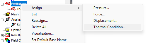
Excitations and Boundary Conditions in AEDT Mechanical
Unlike HFSS, the Mechanical solver does not require an air region around the model. Instead, you apply boundary conditions and excitations directly to the structure. Common excitations include:
-
Pressure
-
Force
-
Displacement
-
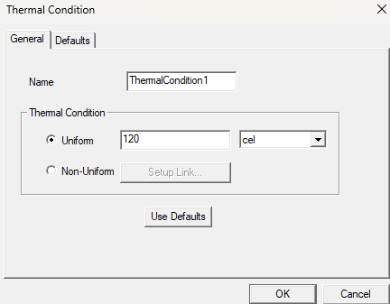
Thermal load
In many electronic applications, thermal load is the most important factor, as temperature cycling drives mechanical stress and raises long-term reliability concerns.
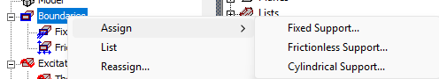
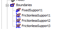
Boundary Conditions
AEDT provides several boundary condition types for mechanical constraints:
-
Fixed support: No displacement in any direction.
-
Frictionless support: Movement is restricted normal to the surface, but tangential sliding is allowed.
-
Cylindrical support: Radial and tangential constraints applied to cylindrical surfaces.
The choice of boundary conditions has a strong impact on the predicted stress and deformation, and should reflect the actual physical mounting of the PCB or package.
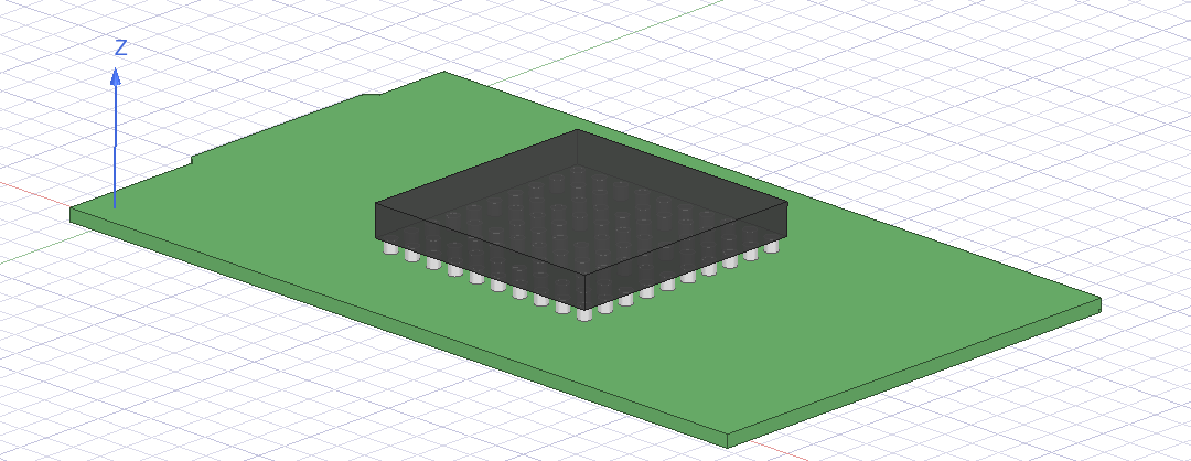
Example: PCB with Die and Solder Pillars in the AEDT Mechanical Solver
Consider a simple package assembly:
-
A PCB substrate,
-
A die mounted on top,
-
Solder pillars connecting the die to the board.
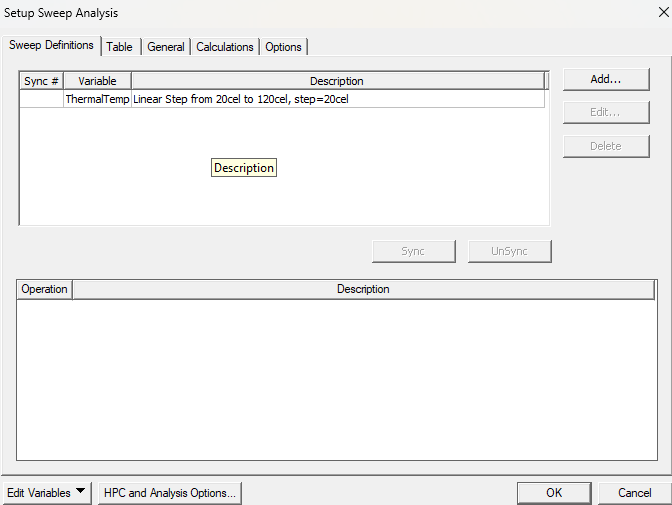
In a mechanical simulation, you assign appropriate materials (e.g., FR4, silicon, SAC solder) and define the initial geometry. Thermal load is applied by sweeping the temperature from 20 °C to 120 °C.
Simulation Workflow: Setting Up an AEDT Mechanical Analysis
-
Geometry creation: Import or build the PCB, die, and solder geometry.
-
Material assignment: Assign proper elastic and thermal properties to each body.
-
Excitations: Apply a thermal sweep (20 °C → 120 °C).
-
Boundary conditions: Apply fixed or frictionless supports at board edges or mounting points.

-
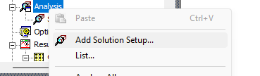
Solver setup: Define a mechanical solver in the analysis tree.
-
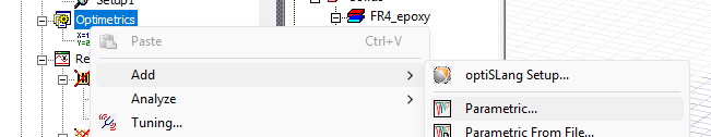
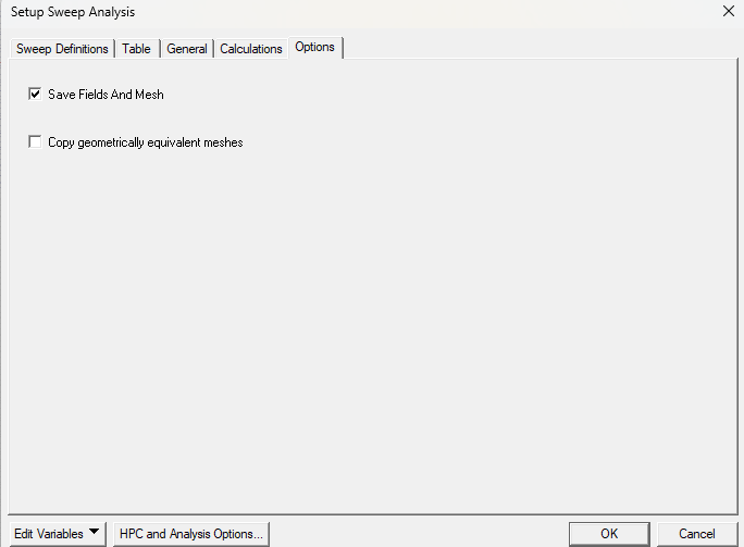
Parametric sweep: Use Optimetrics to sweep temperature and capture deformation/stress at each step.
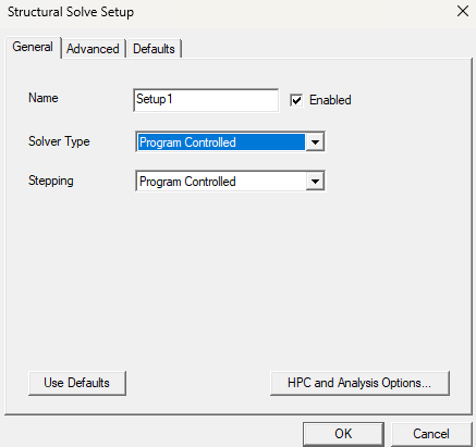
Now the model is ready to be solved
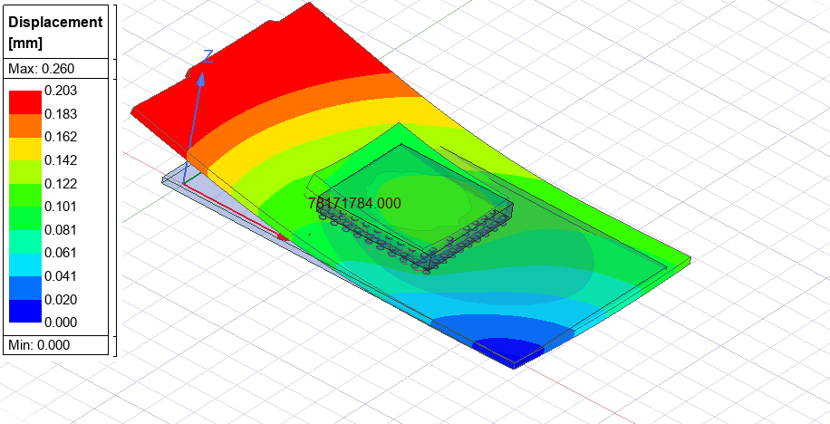
Results: Stress, Strain, and Warpage from the AEDT Mechanical Solver
The outputs of an AEDT mechanical analysis include:
-
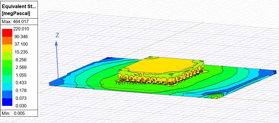
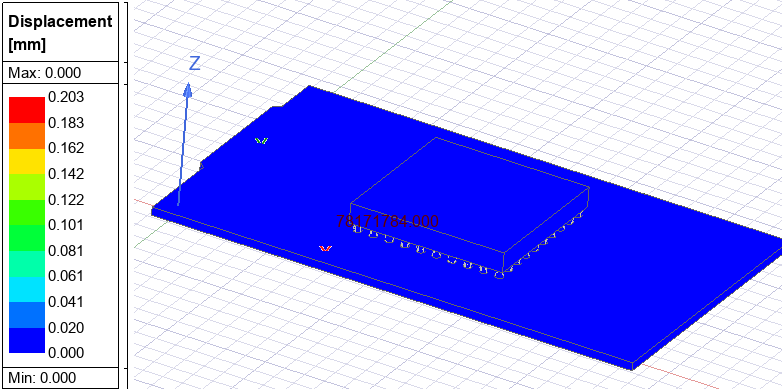
Stress distribution plots: Show where maximum stresses occur in solder joints or die corners.
-
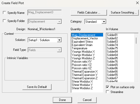
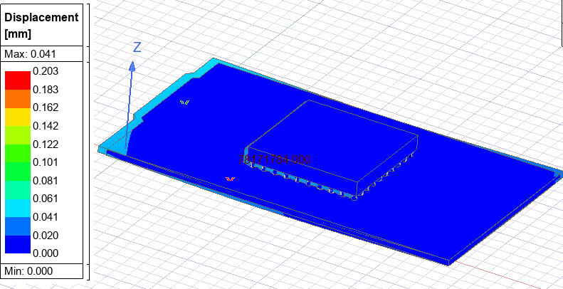
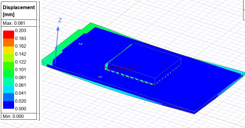
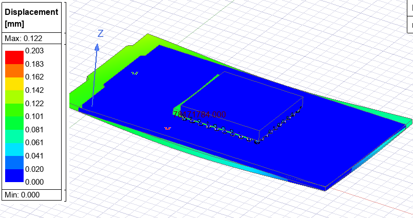
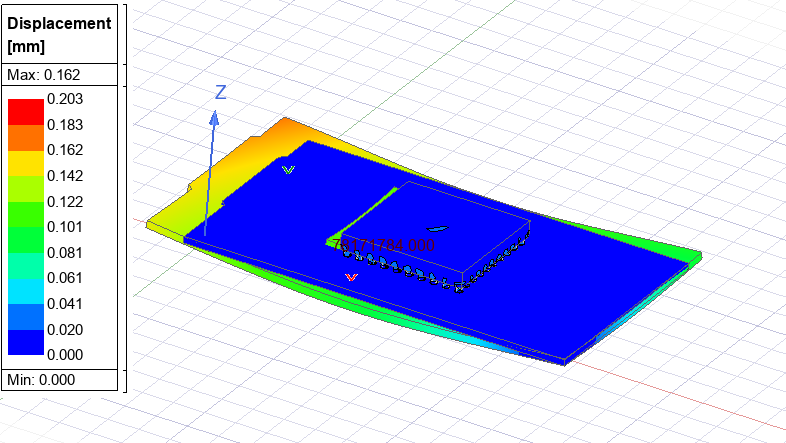
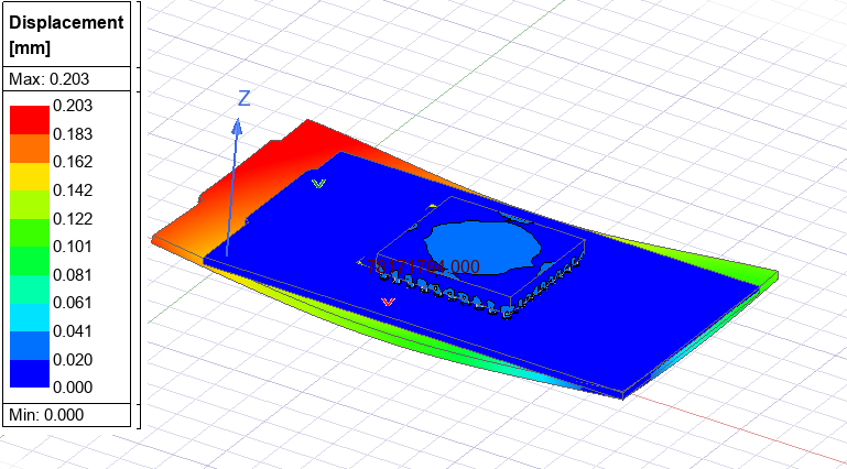
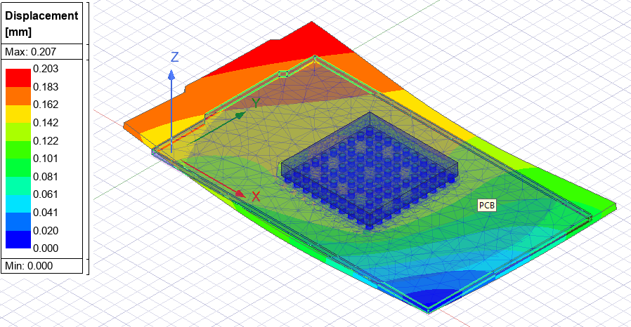
Strain maps: Indicate relative deformation. Select all objects, then plot the displacement
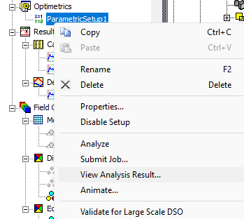
Then right-click the parametric sweep and select Show Results
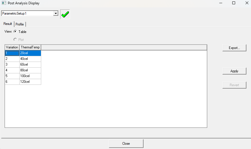
Select 20cel and apply
Select 40cel and apply
60, 80, 100, then 120
-
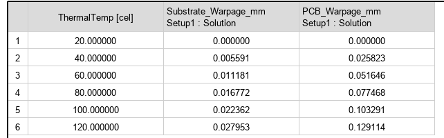
Warpage vs. temperature curves: Help assess risk of board/package bending.
-
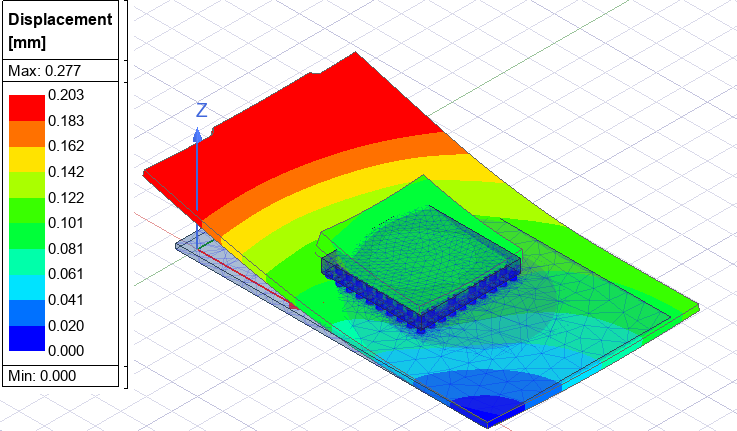
Effect of supports: Changing constraints (fixed vs frictionless) shows how mounting conditions alter stress and warpage. Reduce the number of Frictionless restrictions to 2, 1, then 0 (none) at 120cel:

Key Takeaways: AEDT Mechanical Solver Capabilities for RF Engineers
AEDT Mechanics extends the simulation environment beyond electromagnetic effects to include thermal and mechanical reliability analysis. With the same familiar interface, engineers can:
-
Apply loads (thermal, force, displacement, pressure),
-
Use realistic boundary conditions,
-
Run parametric sweeps over temperature,
-
Visualize stress, strain, and warpage.
This makes AEDT a powerful single environment for evaluating not only electrical performance but also the mechanical robustness of modern electronic assemblies.
Evaluating the mechanical reliability of PCB assemblies or electronic packaging? SimuTech Group’s electromagnetic simulation consultants work with Ansys AEDT, HFSS, SIwave, and the full electronics simulation suite. For more on signal integrity and electromagnetic analysis, see our article on 650+ signal integrity standards for SIwizard in Ansys SIwave. Learn more about Ansys HFSS or contact us to discuss your project.