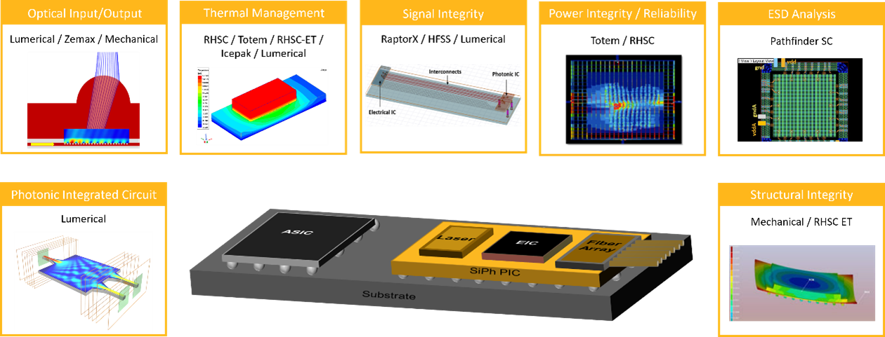
Introduction to Interoperable Photonics Design
Quantum technologies are accelerating rapidly, driven by breakthroughs in molecular modeling, materials discovery, cybersecurity, and next-generation computing architectures. As quantum systems transition from research environments into engineered products, photonic integrated circuits (PICs) have become critical building blocks — enabling stable qubit control, high-precision signal routing, and scalable architectures.
Designing these systems requires more than optical simulation alone. Engineers must consider electrical, thermal, mechanical, and packaging-level interactions to ensure stable operation under real-world constraints. In this blog, we explore how interoperable workflows across Ansys photonic, electrical, mechanical, and thermal solvers enable robust, end-to-end modeling for quantum photonics.
Quantum Photonics: Core Building Blocks
Quantum photonic chips typically integrate four essential device categories:
1. Sources and Lasers
These provide the optical carriers used for qubit encoding, amplification, and readout. Engineers often characterize:
- Mode profiles and confinement
- Effective and group index
- Gain and spontaneous emission
- Temperature-dependent LI curves
- Self-heating and Thermal-threshold behavior
Using Ansys Lumerical MODE, CHARGE, and INTERCONNECT, designers can simulate waveguide modes, solve semiconductor carrier transport, and assemble compact models for circuit‑level sweeps.
2. Passive Photonic Components
Waveguides, MZIs, filters, and ring resonators shape and route optical quantum states. Typical analyses include:
- 2D cross‑section mode solving
- 3D FDTD propagation
- Transmission, reflection, insertion loss
- Extinction ratio and free spectral range
Parameter sweeps and optimization allow rapid design of device geometries such as coupler lengths, interferometer arms, and ring radii.
Intermediate field data and phase information for custom post-processing.

Like what you’re reading? Watch the Interoperable Photonics Design on-demand webinar.
Go deeper into interoperable photonics design with our on-demand webinar, “Interoperable Photonics Design for Quantum Applications using Ansys Simulation Software.” In this session, you’ll see how Ansys Lumerical supports PIC components such as laser sources, modulators, detectors, and I/O couplers, and how seamless multiphysics interoperability enables electro-optical signal integrity analysis, chip-level thermal management, and mechanical stress evaluation across quantum photonic systems.
3. Active Components
Phase shifters and modulators enable device tuning, compensation for fabrication variability, and dynamic reconfiguration. Using Lumerical’s multiphysics solvers, engineers can model:
- Thermo‑optic tuning
- P‑N and P‑I‑N junction carrier effects
- Voltage‑dependent refractive index changes
- Nonlinear materials and carrier‑induced absorption
By combining CHARGE simulations with FDTD and circuit modeling, designers can evaluate resonant peak shifts, tuning efficiency, and bandwidth limitations.
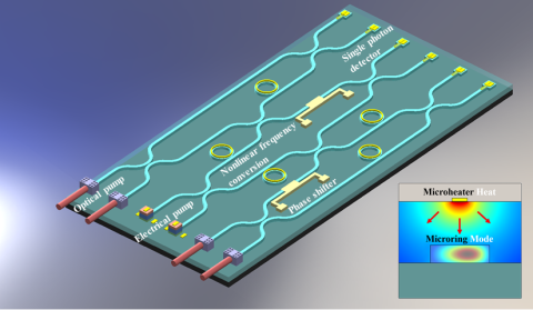
4. Detectors & Ion Traps
Quantum readout requires integrated detectors or ion trapping structures. More advanced workflows pair Lumerical FDTD with Ansys Maxwell to co‑design electrode geometry and optical trapping patterns.
Engineers can:
- Define RF electrode fields for ion stabilization
- Optimize grating coupler far‑field projections
- Evaluate trap symmetry and optical force vectors
- Simulate multi‑beam optical tweezer configurations
This multi-solver approach ensures mechanical forces and electrical fields align with optical trapping requirements.
Multiphysics Integration: Beyond the Photonic Chip
As quantum devices mature into commercial systems, packaging and environmental considerations begin to dominate performance. Interoperable photonics design workflows built within Ansys allow engineers to model challenges at the system level, including optical alignment, signal integrity, thermal gradients, and mechanical stress.
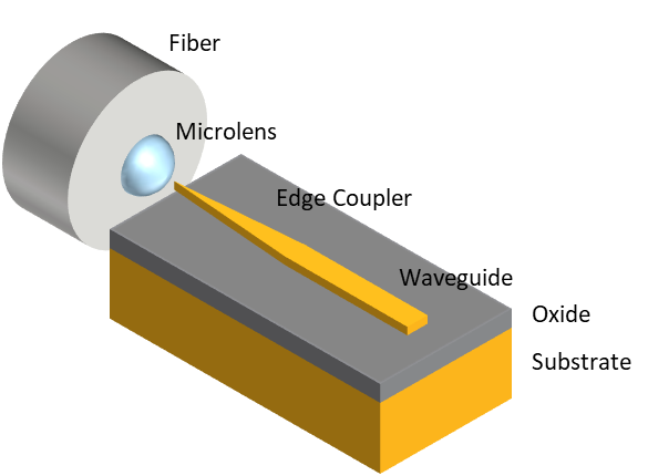
1. Optical I/O Optimization with Lumerical + Zemax OpticStudio
Grating couplers and edge couplers must efficiently interface chips with fibers or free‑space optics. Full 3D simulation of chip‑to‑fiber distance is often computationally prohibitive, so an efficient hybrid workflow is used:
Step 1 — Photonic Simulation (FDTD)
- Optimize grating coupler geometry
- Extract near‑field + far‑field profiles
- Export E‑field distributions
Step 2 — Ray‑Tracing with Zemax
- Import fields into a ZBF source plane
- Model microlenses, fibers, and free‑space gaps
- Run optimization on lens radii & positions
- Quantify lateral alignment tolerances
For example, adding an optimized microlens can increase 3‑dB alignment tolerance from ~7.4 μm to ~22 μm—a 3× improvement in packaging robustness.
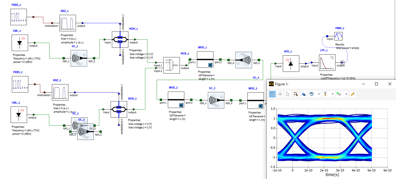
2. Electro‑Optical Co‑Simulation for High‑Speed Links
Quantum control and readout increasingly use hybrid electro‑optic systems. Co‑simulation between Lumerical INTERCONNECT, ANSYS Circuit, and HFSS enables end‑to‑end link analysis:
Workflow Overview
- Electrical Domain (Ansys HFSS):
- Create state space model of interposers
- Circuit design of the driver, routing, and modulator RC
- Output: electrical modulation waveform
- Optical Domain (Ansys Lumerical INTERCONNECT):
- Circuit design using laser, ring modulator, optical loss, and photodetector compact models
- Output: optical eye diagram + photocurrent
- Return to Electrical Domain:
- Circuit design of receiver & load resistor
- Output: Final eye diagram + BER estimation
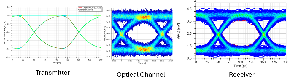
This provides engineers with a true round‑trip analysis of jitter, loss, and signal degradation across heterogeneous domains.
3. Thermal Management Using Icepak + Photonic Compact Models
Quantum components are highly temperature-sensitive—especially resonant modulators and filters. In interoperable photonics design workflows, engineers must analyze temperature-induced spectral drift when chips are integrated near heat-generating electronics.
Workflow
- Thermal Simulation (Icepak):
- Import PCB + IC geometries
- Apply power maps from digital ICs
- Solve 3D steady‑state thermal field
- Optionally build reduced‑order models for speed
- Photonic Simulation (Lumerical):
- Map temperature to compact model or device simulations.
- Update refractive index & resonance shift
- Recompute circuit‑level eye diagrams
This provides engineers with a realistic analysis of signal jitter, loss, and degradation due to temperature.
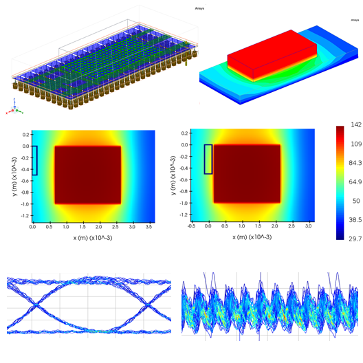
4. Mechanical Stress and Strain in Photonic Devices
Mechanical deformation alters the effective index and physical dimensions of photonic structures. This is especially critical for:
- Bragg gratings
- Fiber‑based sensing systems
- Thermally cycled metal heaters
- Thin‑film waveguides
Lumerical + Ansys Mechanical Workflow
- Run mechanical deformation or bending simulation
- Extract strain distribution along the photonic structure
- Map mechanical strain to the change in refractive index.
- Simulate shifted transmission spectrum in Lumerical
Engineers can obtain insight into transmission shifts due to mechanical effects – critical for packaging stability assessments.
Conclusion
As quantum photonics advances, design challenges extend far beyond isolated optical components. Electrical drivers, thermal environments, packaging tolerances, and mechanical stress all interact with photonic behavior. Interoperable workflows using Ansys solvers allow engineering teams to:
- Simulate from device physics to full system behavior
- Bridge optical, electrical, thermal, and mechanical domains
- Build compact models that scale to complex PICs
- Validate packaging decisions before fabrication
- Accelerate iteration cycles and reduce prototype risk
For teams working on quantum‑enabled hardware, these multiphysics capabilities are no longer optional—they are essential for achieving reliable, manufacturable designs. Interested in applying interoperable photonics workflows to real-world quantum hardware? Explore our quantum hardware expertise or connect with our team to talk through your design goals.