Introduction to PCB Simulation
The increasing complexity of modern wireless RF devices increases the demand for accurate and efficient simulations of large and complex PCB designs. Identifying and predicting potential issues early in the design process saves resources, time, and money. Using Ansys SIwave, engineers can model, simulate and validate high-speed channels and optimize power delivery systems in modern high-performance electronics. SIwave’s full wave extraction of complete power distribution networks (PDN) enables engineers to verify noise margins and ensure impedance profiles are met through automatic decoupling analysis in low-voltage designs.
Overview: Ansys SIwave for Power Integrity
In this blog, we explore how to pinpoint power plane resonances and optimize decoupling capacitor placement using Ansys SIwave. We compare Resonant Mode Analysis and Near-Field Analysis—two powerful approaches to identifying the exact locations within your model that drive impedance issues, ensuring a more stable and efficient design.
Key Takeaways:
- Identify Problem Areas: Learn how to isolate the specific regions where power plane impedance resonances occur.
- Strategic Decoupling: Use simulation data to determine the most effective coordinates for placing decoupling capacitors.
- Workflow Integration: See how these two SIwave techniques complement each other to streamline your Power Integrity (PI) workflow.
Target Impedance
When designing a Power Distribution Network (PDN), the primary objective is to maintain a stable, “flat” voltage supply. This ensures all devices operate within their ripple specifications and receive consistent power across the entire frequency band of interest.
To achieve this, the PDN impedance must remain as low as possible while avoiding high resonances across a broad spectrum—ranging from DC up to the package cut-off frequency. This ideal, maximum allowable impedance value across that frequency range is known as the target impedance.
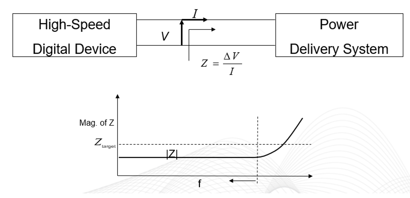
If resonances appear, design modifications become essential to maintain stability. A primary strategy for suppressing these impedance spikes or shifting them beyond the frequency band of interest is the strategic integration of decoupling capacitors. This blog is designed to guide you through the simulation-driven process of identifying the locations within your model where these capacitors will provide the maximum benefit.
To calculate the impedance, the Ansys SIwave workflow wizard can be used to access the Configure PI Analysis dialog box and quickly setup the power integrity simulation. We will be analyzing the 1.2 V power net, which is supplied by a DC-DC regulator. Once the net is selected from the left box, the right box will be populated with all the connections. The user specifies the location of the ports.
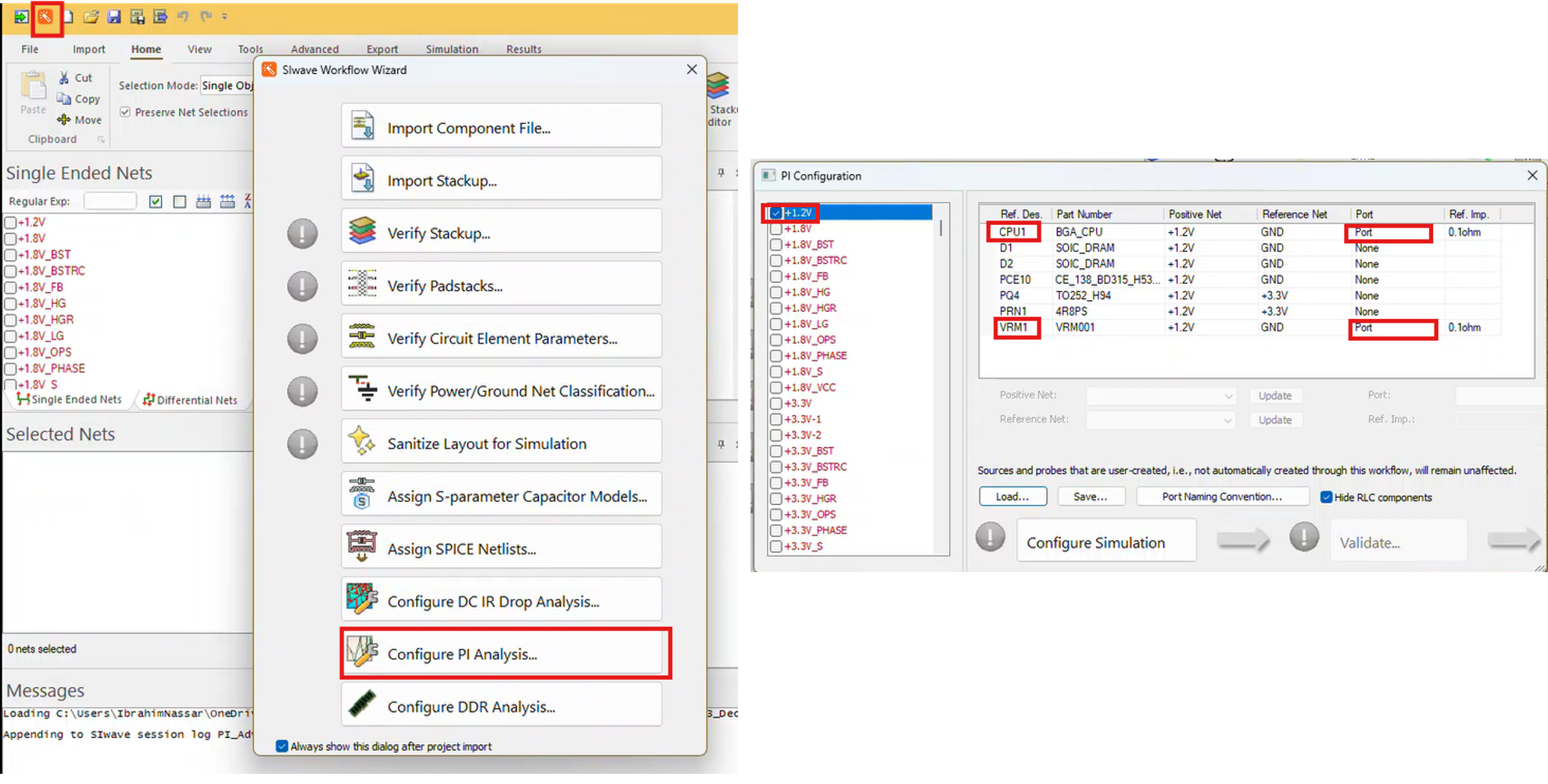
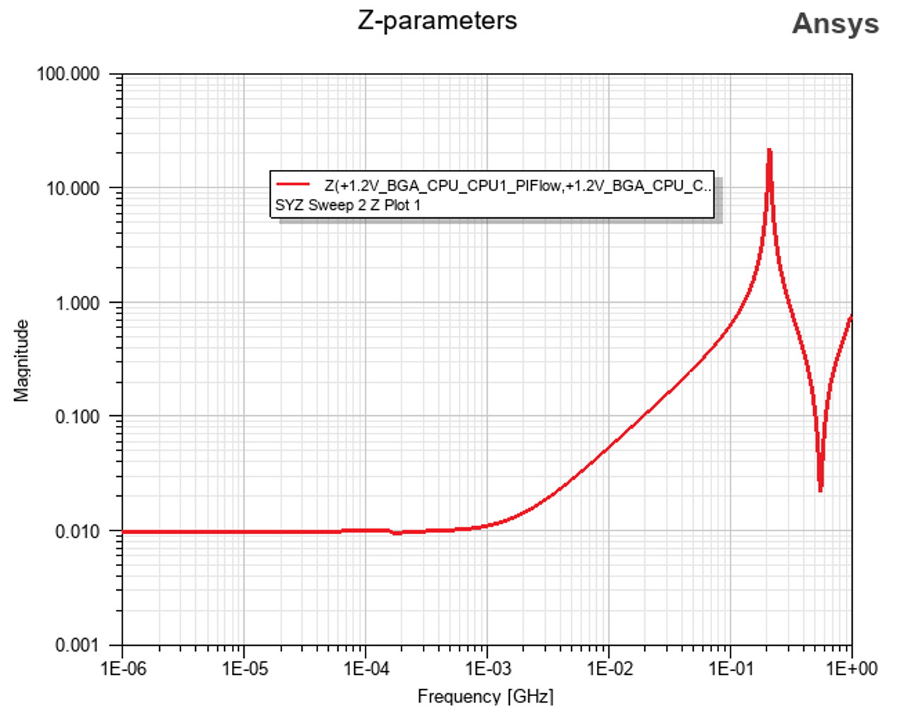
To be able to extract Z11 or input impedance looking into the 1.2V PDN, we can terminate the VRM and keep the port on the CPU power pins. Based on the VRM data sheet, the VRM should be terminated with a 0.47 nH inductor and 0.008 ohm resistor. Below is the simulated impedance looking into the VRM, using the SYZ solver. We clearly see a high resonance occurs near 200 MHz. High resonance indicates the potential for a high voltage drop to be produced on the power plane as a result of transient currents.
Resonance Mode Analysis
In our Ansys SIwave power integrity simulation example, the resonant mode analysis is based on a 2D Eigen mode calculation. It calculates the natural resonances in the cavities formed between board layers. These resonances correlate to peaks in the impedance response. Based on the simulated Z11, we clearly see high resonance near 200 MHz. Using the resonant mode analysis, we will identify where in the model this resonance occurs to help us determine where to place decoupling capacitors to suppress this high peak.
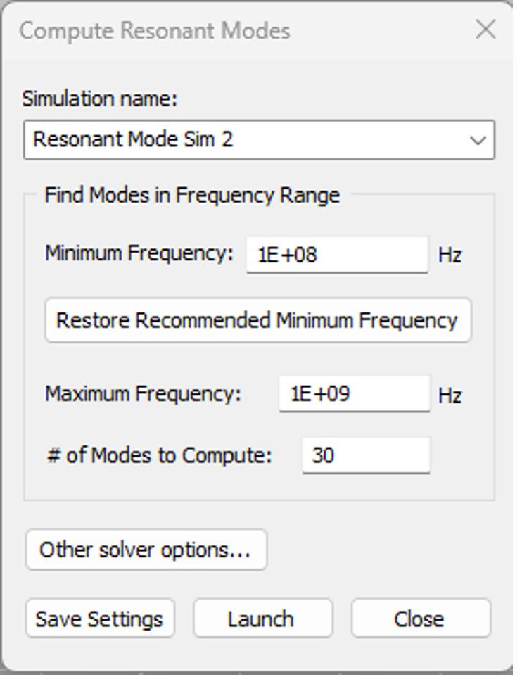
Setting up the resonant mode analysis is very simple. The user needs only to enter the min/max frequency of interests and the number of modes, as seen in the below figure.
Once the simulation is complete, the user gets a list of all the calculated resonances in the PCB within the defined frequency range. The real part represents the resonant frequency, and the imaginary part stands for the losses of the resonance or the decay factor. The value of k is the eigen number, equal to the resonance frequency times 2PI/ speed of light in free space, and it is around 20.954 times the resonant frequency in GHz. The wavelength is the wavelength at the resonance in air, and Q is a measure of how sharp the resonance is, and it is equal to the resonant frequency/ 2 times the imaginary part.
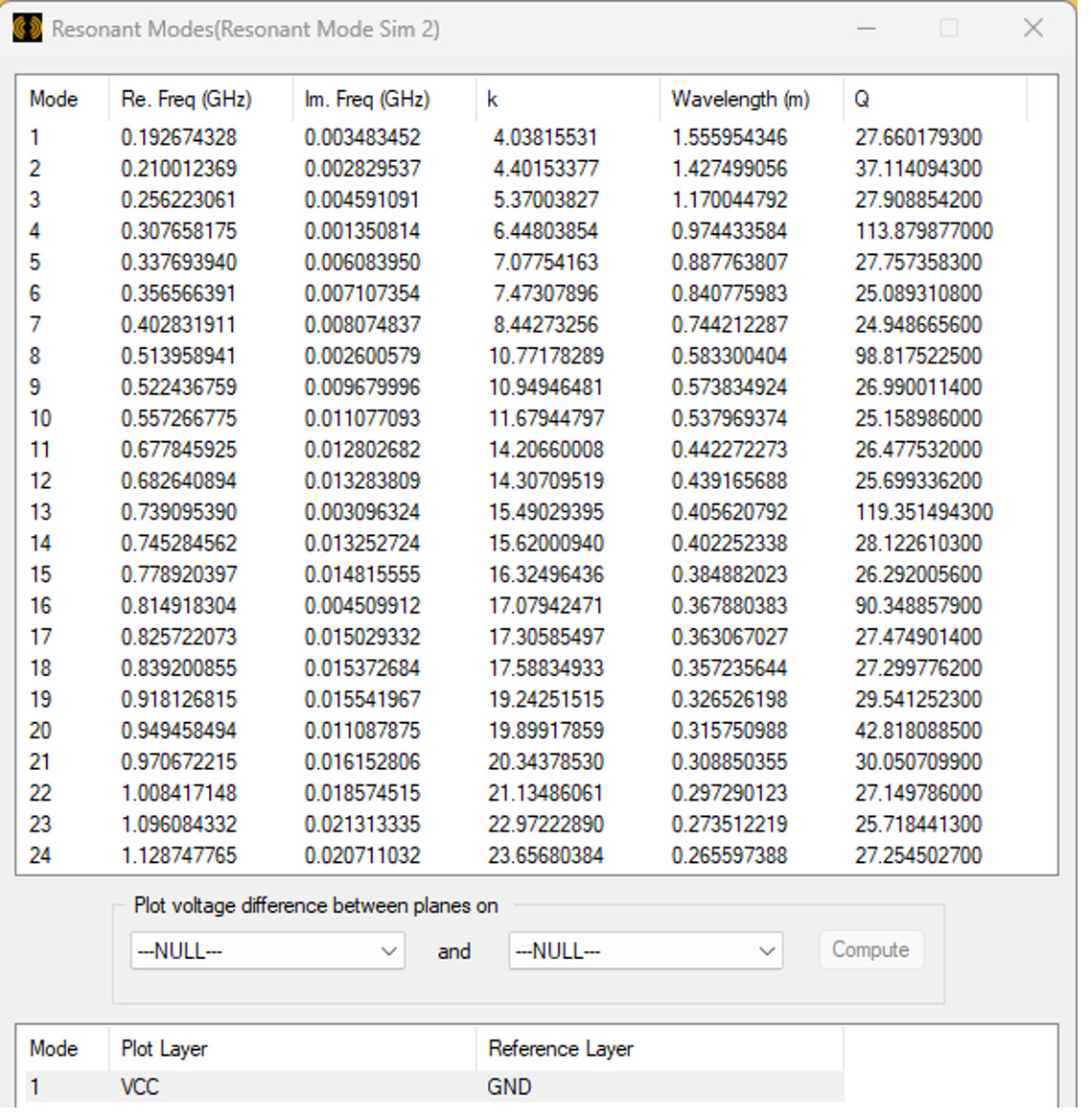
It is important to understand that the resonance exists between planes. SIwave plots the resonance between layers only. The user needs to select to plot the voltage between two layers: the one where the power planes are located and its return plane. Some of these resonances are strong, and others are weak. However, we should be concerned only with the resonance that can be excited.
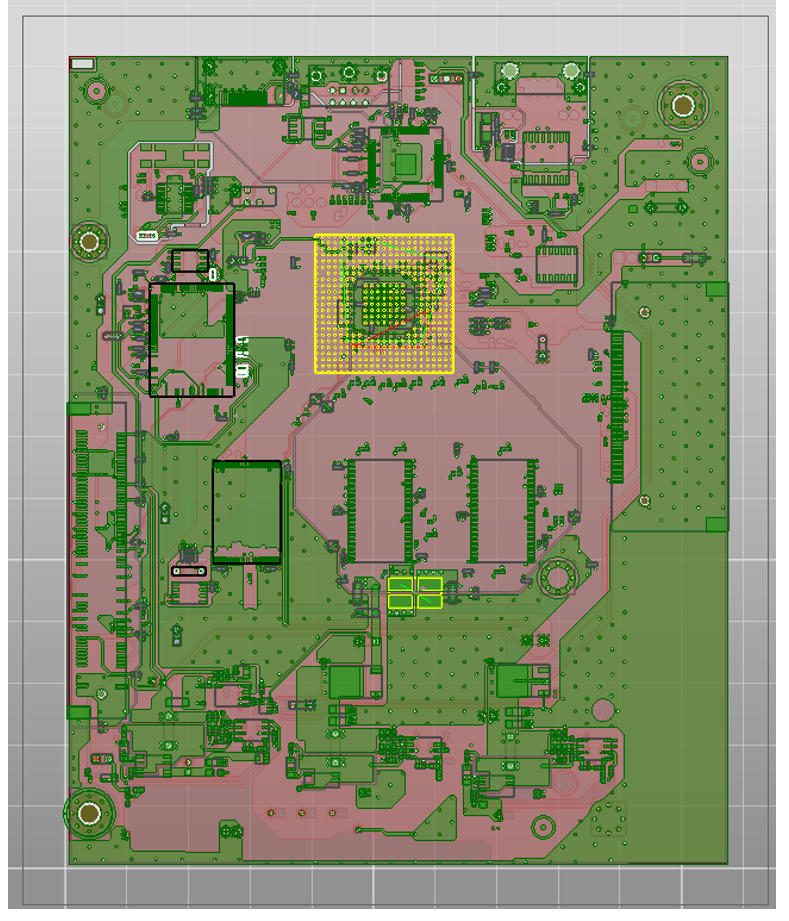
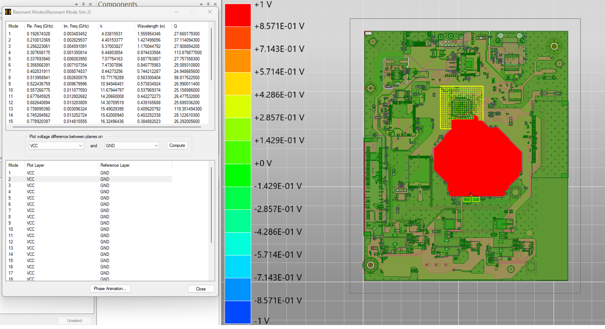
Based on the Z11 data, the resonance occurs near 200 MHz for the 1.2 V power plane. This means that the second mode is the one that can be excited and based on reviewing all the layers, it will exist between the VCC and the GND plane. Below is the field plot, and we clearly see where high voltage can exist. The ideal location for capacitor placement is made evident from the voltage distribution plot provided in Figure 7 below. After adding the capacitors, we can re-run the simulation to verify if the resonance is suppressed.
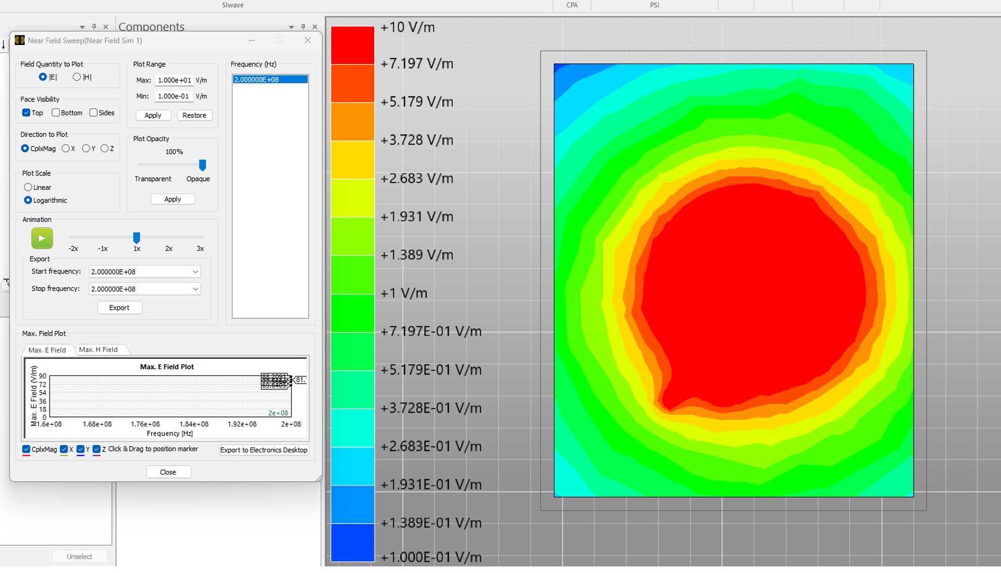
Near Field Analysis
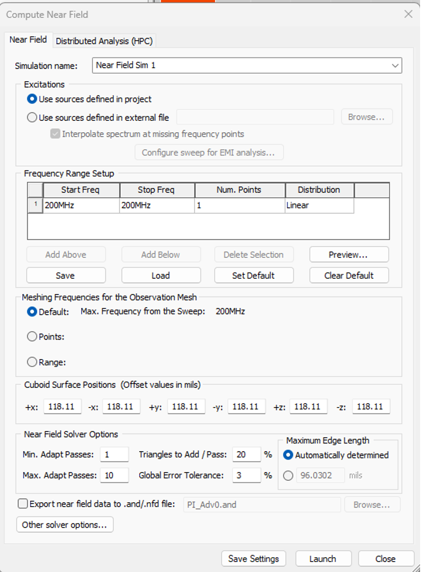
Ansys SIwave has an integrated near field solver that can be used to simulate emissions off board. In this particular power integrity example, we will use this solver to identify the region in the model with high electric field intensity. To setup the near field analysis, we need to place a voltage or current source at one side and a termination (high impedance) at the other side of the power plane, the VRM in this example.
Below is the Near Field window setup. As seen, the near fields will be calculated at 200 MHz, the frequency at which the impedance was found to be high.
Below is the Near E field plot at 200 MHz. As seen, we clearly see high E field magnitudes in the middle region. This result agrees with the resonant mode analysis.
Ansys SIwave Power Integrity Analysis: In Summary
In this blog, we have demonstrated how Resonant Mode Analysis and Near-Field Analysis function as two powerful, complementary workflows within Ansys SIwave. Both methods effectively pinpoint the “hotspots” where power plane impedance resonances originate. Because both approaches yield consistent, high-fidelity results, designers can have greater confidence in their PDN design decisions.
Comparison of the Two Approaches:
- Resonant Mode Analysis: Offers a global view of the PCB, identifying the specific frequencies and physical modes that trigger voltage fluctuations.
- Near-Field Analysis: Provides a detailed look at the electromagnetic fields (E and H) surrounding the planes, visualizing the areas of high intensity that require mitigation.
- Consistency: The fact that both tools provide similar results validates the simulation strategy, ensuring you are targeting the correct regions for decoupling.
Continue Learning in SimuTech SkillsCenter
Want to see the full workflow in action? Watch the related SkillsCenter recording in the SimuTech Customer Center to learn more about using Ansys SIwave for power integrity analysis, impedance extraction, and decoupling strategy.

Ibrahim Nassar, PhD
Lead Engineer – RF/Microwave, SimuTech Group
Ibrahim Nassar, PhD, is a Lead Engineer – RF/Microwave at SimuTech Group. He has 15+ years of experience in RF/Microwave and antenna design, complemented by a strong background in Power and Signal Integrity (PI/SI) analysis. He specializes in antenna, RF, microwave, and electromagnetic design, with experience in antennas and propagation, wireless sensing, harmonic radar, compact antenna design, and high-frequency electromagnetic simulation.